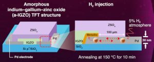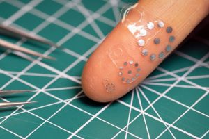
In particular, they are amorphous indium gallium oxide (a-IGZO) thin-film transistors that are being proposed for a form of DRAM, where memory density can be increased by stacking the transistors.
The problem is that the resistance of the interface between metal electrodes and the IGZO channel can be excessive.
It is known that introducing hydrogen into the interface can make changes that permanently reduce this interface resistance, and ways to diffuse the gas down through upper layers to the interfaces have been found previously, according to Tokyo Tech, but they are multi-step processes, and are impractical with stacked thin-film transistors.
The Tokyo team picked palladium as the source and drain contact metal, which is unusually good at absorbing hydrogen in between its atoms.
So long as the electrodes come to the surface of the layers somewhere near the transistor, the palladium acts as a wick, conducting hydrogen to the crucial interfaces from the inside the metal.
“This method requires a metal that has a high hydrogen diffusion rate and hydrogen solubility to shorten post-treatment times and reduce processing temperatures,” said researcher Masatake Tsuji, of Tokyo Tech’s MDX Research Center for Element Strategy. “We utilized palladium as it fulfills the dual role of catalysing hydrogen dissociation and transport, making it the most suitable material for hydrogen injection in amorphous oxide semiconductors at low temperatures, even at deep internal contacts.”
In a proof-of-concept, IGZO thin-film transistors with thin-film palladium electrodes were fabricated, and heat-treated at 150°C for 10 minutes in a in a 5% hydrogen atmosphere.
“Testing revealed that contact resistance of the TFTs was reduced by two orders of magnitude. Moreover, the charge carrier mobility increased from 3.2cm2/V/s to nearly 20cm2/V/s,” according to the university. “Additionally, this method preserved the stability of the TFTs, suggesting no side effects due to hydrogen diffusion in the electrodes.”
As an aside, the team picked ZnO-SiO2 as a passivation layer over the transistors for its ability to block impurities and water from from the channels, and also to block hydrogen so that the palladium was the only route to the interface.
The work is published as ‘Approach to low contact resistance formation on buried interface in oxide thin-film transistors: utilization of palladium-mediated hydrogen pathway‘ in ACS Nano.
 Electronics Weekly Electronics Design & Components Tech News


